Our process technology is characterised by customised, efficient concepts made up of tried-and-tested modules.
We offer customised automation solutions that are precisely tailored to customer requirements.
Our service, maintenance and training services are customised to your individual needs.
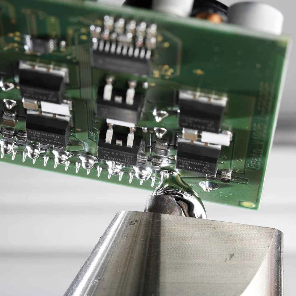
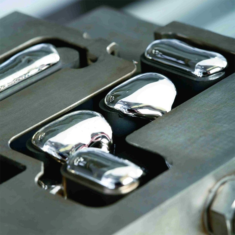
The selective solder wave presented at Coiltech guarantees a soldering process free of oxides and residues thanks to the inert gas atmosphere. The solder wave, which is continuously pumped by an induction pump, transfers the heat transfer from the molten solder homogeneously and circumferentially to the solder joint geometry. The flowing solder wave cleans the solder joint of excess flux residue, oxides and dirt.
The solder joint is physically self-adjusting due to the capillary filling level solder saturation. The optimum solder geometry is reliably mapped to the pad pin mould, pin hole position and thermal mass distribution in the PCB structure. Solder crossings, menisci and intermetallic phase characteristics round off the overall performance in a reproducible manner.
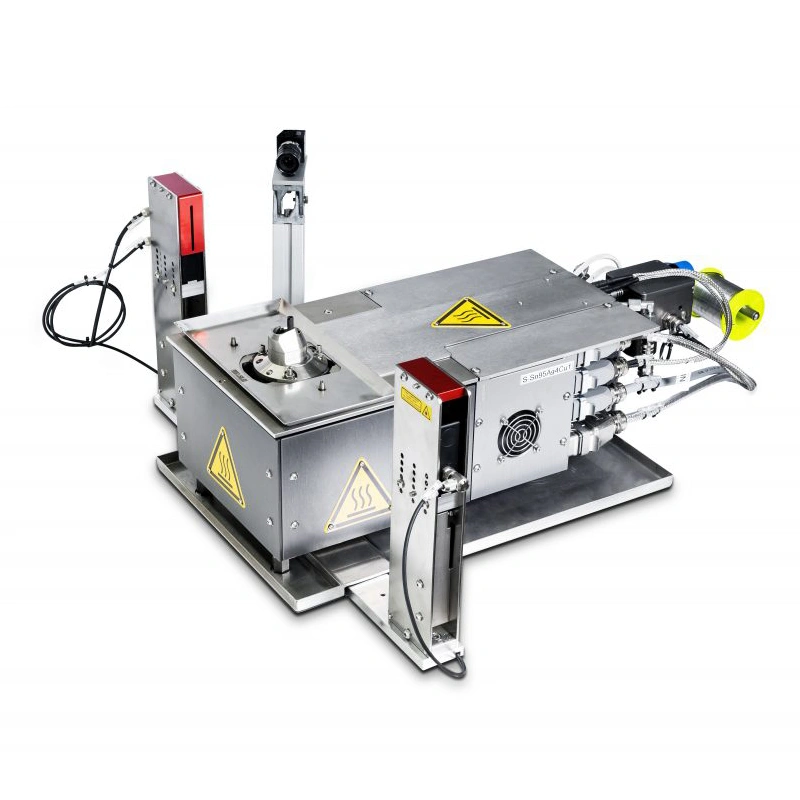
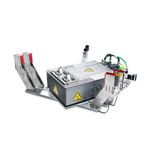
The modular solder tank sizes together with the electromagnetic solder pump system and the quick-change solder nozzles form the basic process module. The redundant temperature control, the constant solder bath level, the optional solder wave height control and the continuous solder wire tracking guarantee maximum system autonomy.
In conventional wave soldering, a large area of the printed circuit board is passed through a wave of solder at the same time. In the Mini wave soldering In contrast, soldering is carried out selectively and locally. This allows individual pins, groups of pins or defined areas to be soldered without subjecting neighbouring components to unnecessary thermal stress or bringing them into contact with the solder.
Selective soldering is the umbrella term for soldering processes in which individual solder joints or areas of an assembly are targeted for processing. The Mini wave soldering is a form of selective soldering. In this process, heat and solder are transferred via a locally confined, continuously fed wave of solder.
Mini wave soldering It is particularly suitable for printed circuit boards with THT components, mixed assemblies comprising THT and SMT components, and for assemblies with complex geometries or high requirements in terms of process reliability. Thanks to customised solder nozzles Even solder joints that are difficult to access or are close together can be worked on with precision.
Key advantages include high and reproducible solder joint quality, controlled solder flow, low solder consumption and high process reliability. At the same time, the thermal stress on the assembly and contact between the solder and areas not to be soldered can be reduced. The process can also be easily automated and integrated into various manufacturing concepts.
A nitrogen or inert gas atmosphere reduces oxidation during the brazing process. This helps to ensure stable process conditions and a high standard of wetting. At EUTECT, the brazing process is carried out in an inert gas atmosphere to minimise oxides and residues during selective brazing.
The geometry of the solder nozzle has a significant influence on how the molten solder is directed to the solder joint. It must therefore be tailored to the component geometry, pin arrangement, printed circuit board design and the specific process. EUTECT uses custom-designed solder nozzle geometries to enable reproducible solder flow and targeted heat transfer.
The Induction pump ensures the continuous feed of the liquid solder to the solder nozzle. With EUTECT technology, the pump system operates electromagnetically and requires no mechanically moving parts within the solder. This ensures a reproducible solder flow as well as a low-maintenance and stable soldering process.
Consistent solder joint quality is achieved through the controlled interplay of solder temperature, solder wave height, Nozzles- and Mask geometry, process time, inert gas atmosphere and the positioning of the assembly. At EUTECT, process stability is supported by, amongst other things, redundant temperature control, a constant solder bath level and, optionally, solder wave height control.
With appropriately designed solder nozzles Individual solder joints, as well as several pins or defined soldering areas, can be processed. The nozzle geometry is adapted to the specific application. This means that mini-wave soldering can be used for both spot soldering tasks and more complex THT connections.
Controlled heat transfer and continuous contact with the solder wave can help to ensure reproducible solder penetration. Key factors here include, amongst others, pin and hole geometry, thermal mass, PCB design, flux and the selected process parameters.
Yes. Mini wave soldering It is suitable for automated electronics manufacturing and can be integrated into a variety of machine and automation systems. Depending on the assembly, production volume and cycle time requirements, motion sequences, workpiece handling and process monitoring can be tailored to the specific manufacturing task.
The cycle time depends, amongst other things, on the number and arrangement of the solder joints, the Nozzle shape, the required heat input, the movement sequences and the Automation concept . Through an application-specific design of solder nozzle, Workpiece carrier, By adjusting the process parameters and kinematics, the soldering process can be specifically optimised to achieve short and reproducible cycle times.
Key factors include the geometry of the solder joints, pin and hole diameters, PCB design, thermal masses, component spacing, the solder alloy and flux used, and the required cycle time. In addition, the following must solder nozzle, Workpiece carriers, masking, temperature control and the automation concept must be coordinated.
In automated soldering systems, relevant process parameters can be monitored, documented and assigned to a product or assembly. This enables process flows to be traced and supports traceability and quality assurance requirements.